Description
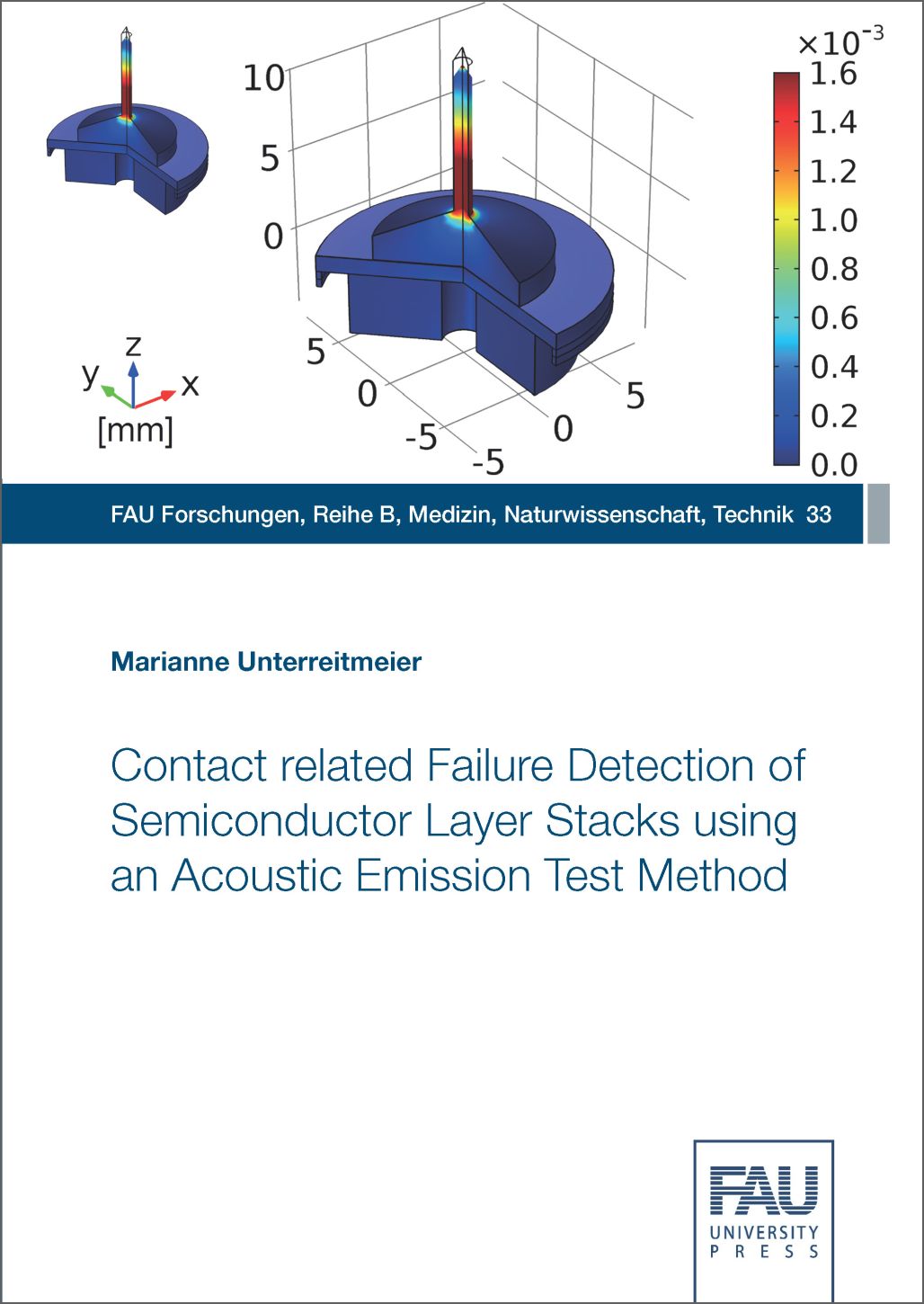
The book provides the reader with a novel, non-destructive test method for mechanical damages in semiconductor structures that can arise when contacting connection pads of integrated circuits during probing on wafer level. Instead of time-consuming and costly failure analyzes using optical and electrical methods, an acoustic emission test method is presented, which was adapted and optimized to the application case wafer test. The system was simulated using suitable models and verified in extensive experiments on suitable test structures. Based on detailed explanations, mathematical derivations of the micromechanical stress and frequency response states, precisely illustrated figures and numerous high-quality optical pictures, a well-founded elaboration of the problem and solution of a newly developed sensor-indenter system for thin layer crack detection is presented. All chapters have an introduction overview and a summary of the main results and conclusions. The work thus makes a significant contribution to reducing development costs and increasing the reliability of complex semiconductor structures of current and future technologies.


Reviews
There are no reviews yet.